Additionally, the
reliability characteristic is of crucial importance in today's High Performance and Energy Efficient Computing (HPEEC) applications since the malfunctioning of a component results in lower performance and waste of energy.
Therefore, similar to any new technology the reliability of the proposed communication methodologies is a crucial issue.
Although many general
analysis tools have been presented especially for investigating the reliability properties of the processors, these tools are not accurate enough to reveal
fault tolerance characteristics of the next generation on-
chip communication links.
However, the first two factors have already reached their limits.
The problem of process technology scaling is more related to wire issues and
energy consumption concerns rather than the device design challenges.
In addition, technology and supply
voltage scaling slows down due to physical limitation in
nano fabrication feature size.
With each passing year, the number of problems where experiments are impossible, dangerous, or inordinately costly is growing.
The other
advantage of many-core design is increasing the raw performance by enhancing the
clock per instruction factor rather than frequency, which consequently results in slower growth in
energy consumption.
Therefore, many-core architecture manifests a good tradeoff between technology scaling and limited energy budget requirement.
The reason is that the wire delays have become more critical in smaller feature size, as technology scaling results in larger
capacitance for global wires.
Therefore, global wires are not scalable in terms of
delay, energy consumption, and bandwidth.
In addition, global clocking is another challenge in traditional
bus-based interconnections.
The
clock tree method has been suggested to resolve this issue, but it consumes large portion of energy and area budget.
It should be also added that a
bus-based
system has a limited capability of concurrent communication.
Moreover, buses broadcast the data to transfer them among the cores in which the entire
bus wires should be switching from on to off state periodically; resulting in large waste of energy.
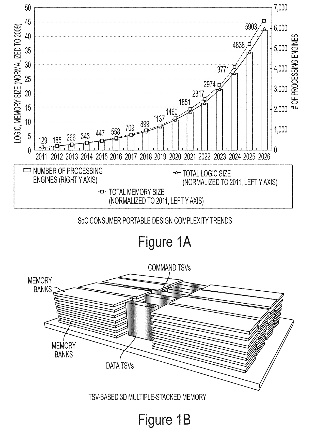
On the other side, 3D NoC architectures demand many trade-offs in order to meet some specific performance requirements, which results in various design issues.
Shrinking
transistor sizes, smaller interconnect features, 3D packaging issues, and higher frequencies of
CMOS circuits lead to higher error rates and more thermal and timing violations.
However, none of them protect faulty
datapath inside routers.
Also, there is no measurement capability to compare the effectiveness of the proposed reliable 3D NoC architectures.
An analytical model for reliability evaluation of 2D NoC can be presented, but it is not reusable for 3D die-stacking designs in which new sources of faults are presented.
Many major reliability issues are presented by the emergence of 3D structures such as thermal concerns and TSV issues as a result of 3D structures.
The unwanted
heat generation by PEs in 3D NoC should be removed effectively otherwise it may result in other problems.
These effects are different from the traditional
crosstalk issues due to differences between the physical characteristics of TSVs and 2D wires.
Additionally, the generated
noise signals by TSVs, may also have undesirable effect on the performance of 2D components such as transistors or 2D wires.
Furthermore, there are still additional issues for developing 3D architecture EDA tools.
On the other hand, measurements are expensive and
time consuming while time-to-market cycle is of great importance.
Consequently, developing general analytical techniques to advance both the intuitive understanding and the quantitative measurement of how potential physical faults influence the behavior of 3D NoC are still lacking although many researches have focused on reliability issues for 3D NoC architectures.
This tool can be applied investigating the capability of proposed fault-tolerant 3D NoC approaches at the early stage of the design, which saves both time and cost of design.
By comparing the value of selected signals and their assertion time in 3D NoC components after running both faulty and faultless experiments the
vulnerability of each component is reported.
Although the experimental process in this method is fast, but the experimental set up is
time consuming.
In addition, this method needs the actual hardware in order to run the
fault injection process, resulting in a costly method.
Comparing to physical-based fault models they do not need the actual model of the
system, but they have some limitation in terms of
fault injection coverage and
observability.
However, none of the existing tools are efficiently reusable for 3D NoC platforms, since 3D NoCs are susceptible to different fault sources that are not fully addressed by existing tools like 3D design issues.
Furthermore, components and behavior of a 3D NoC is different from other computational platforms.
ARROW is the only fault
injector tool for NoC platform, which only supports 2D NoC design and it does not provide any reliability analysis.
This is critical since based on our experiments; random fault injection may result in 26%-99% inaccuracy of reliability evaluation process.
To guarantee the
correctness of computing and communication services of many-core systems, has always been a major challenge for both designers and end users.
A
system may not always perform as it is expected to, because of environmental conditions or internal faults.
Each of these environmental conditions may result in an internal fault and consequently causes other unexpected behavior in the system.
In general, causes and consequences of deviations from the promised functionality of a system are known as
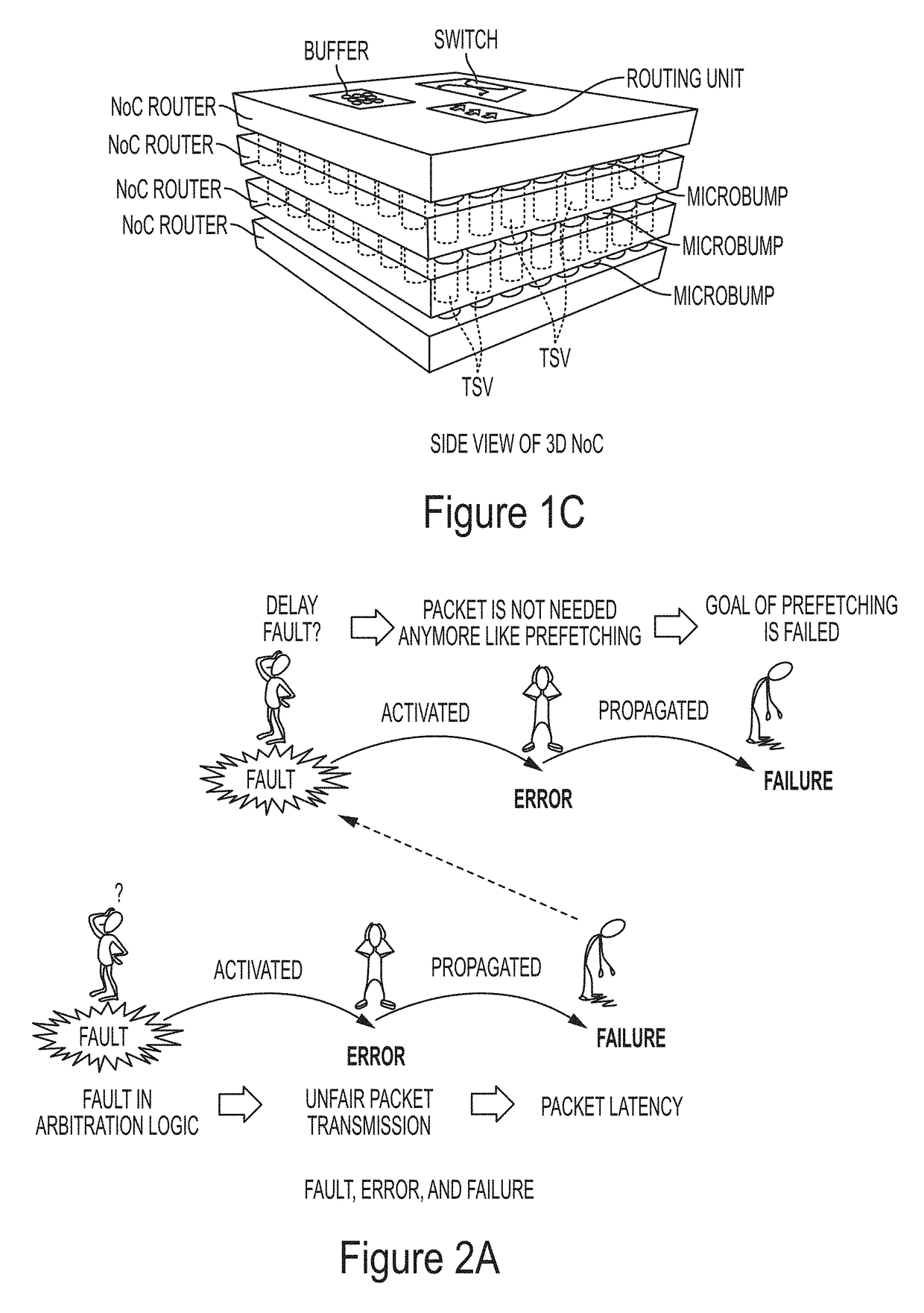
dependability threats including: fault, error, and failure.
Fault is a physical defect, imperfection, or flaw that occurs within some hardware or
software component.
A fault is active when it ends in an error, otherwise it is dormant.
However, a permanent fault exists in the system till the end of system's
life time.
With applying error detection techniques; an error is called a latent one, as long as it has not been recognized, otherwise it remains as latent error in the system.
In addition, a latent error may disappear or be overwritten before it is detected.
But, most often many of the errors are propagated and consequently generate more errors or pass through the system which result in single or more failures.
A failure is the non-performance of some action that is due or expected.
Such as
packet loss in
data transmission because of missing correct data capturing or missing a
software event as a result of regenerating unexpected values are examples of failures.
A component
failure causes a fault for the system which it belongs to or the other components which are interacting with.
If a fault in arbitration component of routing unit is activated; it will generate an unfair
packet transmission through the system which consequently results in a packet latency failure.
This failure can be considered as a kind of delay latency in the
receiver side which is supposed to perform the prefetching operation.
The activation of the delay fault results in an error in which the packet is not needed anymore.
However, if the applied method is not resilient enough to prevent the
fault occurrence, they cannot resolve the issue.
As expected this method cannot resolve the permanent faults.
This method is fast but complex especially as the size of system grows, but the system is simulated and its behavior is evaluated in the presence of faults by running large number of experiments.
In most cases, the expected
dependability is not achieved by using any of them, separately.
This method is expensive and usually is considered at the final stage of
mass production.
This method is much cheaper than hardware-based evaluation and it is considered at the beginning stages of design, but the
simulation-based method takes longer time than the hardware-based one.
In addition, the advent of 3D integration results in considerably shorter interconnects wires in the vertical direction.
There is a tradeoff between the complexity of flow control implementation and its efficiency.
On the other hand, this method has a set-up phase which is not efficient especially for short messages.
The other approach is packet-based flow control which has been proposed due to the inefficiency of
circuit switching method for NoC applications.
This method does not consider the status of the network in choosing the path for incoming flits.
The
disadvantage of this method is that the size of header flit increases for larger network sizes.
Wire-bonding and flip-
chip stacking have made their ways into mainstream
semiconductor manufacturing in recent years, but they are not considered anymore for new generation of 3D integrations.
However, irregular TSV placement results in a critical fabrication issue which is known as chip warpage.
Additionally, TSVs have different characteristics other than 2D wires, resulting in new challenging designs which are discussed in Chapter 4.
But, NEA is not scalable and imposes a large data overhead.
If the size of a flit is large, the
limiting factor in wire routing or bandwidth efficiency parameters is not satisfied.
Any
fault occurrence on the header flit may result in a misrouting of the whole packet.
The extra routing information bits in the header flit which limits the
scalability and decrease the reliability of NoC is the major problem of
source routing methods.
A packet is faulty, if at least one bit is erroneous.
The NEA method is not considered for these evaluation
metrics because of its large design complexity and overhead.
However, total dynamic power consumption of the baseline, the TagNoC, and other
source routing techniques do not increase since they all employ the same buffer, crossbar, and
arbiter components.
But, at the
router level it can be observed that EA / OEA methods consume slightly
higher power than the baseline.
The reason behind this observation is that in EA / OEA methods the number of header bits imposed by the
routing algorithm is more than the baseline method which leads to more power consumption.
With theses features higher error rates are expected and consequently the probability of a chip failure is rising.
Consequently, the
mass production of 3D ICs for
consumer electronic products are not reliable enough without a systematic and thorough reliability assessment.
These advantages may not be completely achieved because of chip warpage, TSV
coupling, and thermal stress as major TSV
failure causes.
Chip warpage: When TSVs are used for vertical interconnects, it may lead to chip damage, since the TSVs are arranged in a non-uniform manner.
TSV-related defects might occur in the fabrication process of TSV placement, in the bonding of the TSVs to the next layer like
wafer warpage.
Although buffer
insertion method has been proposed with the goal of delay reduction, but it imposes extra area and power consumption overheads.
This is because the occupied die area by TSVs is quite significant which in turn compromises the wire length benefit of 3D ICs.
Meaning that, small TSVs have less area overhead, but they cause serious delay overhead.
So, the TSV
coupling is one of the major issues for the future 3D NoC designs.
In more details, TSV
coupling may result in delay because of mutual coupling effects between adjacent TSV pairs.
The thermal stresses can drive interfacial
delamination between the TSV and the Si matrix, damaging the on-chip wiring structures.
It can affect the carrier mobility due to the piezoresistivity and degrading the performance of the
MOSFET devices.
Thermomigration is not a concern in Al and Cu
interconnect technology; but it is now recognized as a serious reliability problem for
flip chip solder joints in 3D packaging.
The majority of power consumption is attributed to transistors, because the resistivity of
silicon is much higher than metals and there are more than a billion transistors on advanced chips.
Furthermore, the heat generated by solder joints is much lower than the
transistor and interconnects metallization; it affects locally the area surrounding (underfill) solder bumps.
The flow of the underfill reduces its role in the protection of the bump as well as the chip.
When the leakage current of
gate oxide reaches its limitation, the breakdown may happen which results in the failure of device.
TDDB has been considered among researchers as a significant failure mode for deep sub-micron technologies.
TDDB is one of the main issues for high temperature in thin oxides.
This stress can cause composition deformation in
metal lines, resulting in short-circuits between
metal lines, or vacancies in the
metal lines causing
creep and converge in a single location which consequently form a void.
It causes cyclic strains and develops cracks in a similar way to natural usage and weakens the joint structure by cyclic fatigue.
The effect of thermal
cycling gets worse in 3D design, since the temperature of different
layers are not the same and there is always a thermal flow between
layers.
SEEs induced by heavy ions, protons, and neutrons become an increasing limitation of the reliability of electronic components, circuits, and systems.
SEE has been the main concern in space applications, with potentially serious consequences for the
spacecraft, including loss of information,
functional failure, or loss of control.
It can be destructive or transient, according to the amount of energy deposited by the
charged particle and the location of strike on the device.
So the current version of TREAT is not able to model dynamic thermal stress and thermal concerns, but they are supported as static fault libraries in the current version of TREAT.
To model the presented faults in Section 4.1.1 at the physical-level, one has to develop an accurate reliability evaluation of 3D NoC, but it is
time consuming as compared to logic-level or higher level modeling.
In addition, the physical-level is not adapted for the
simulation of complex designs such as 3D NoCs because of their long
simulation time.
Activating several of them at the same time results in modeling Multiple Event Upset (MEU) physical faults.
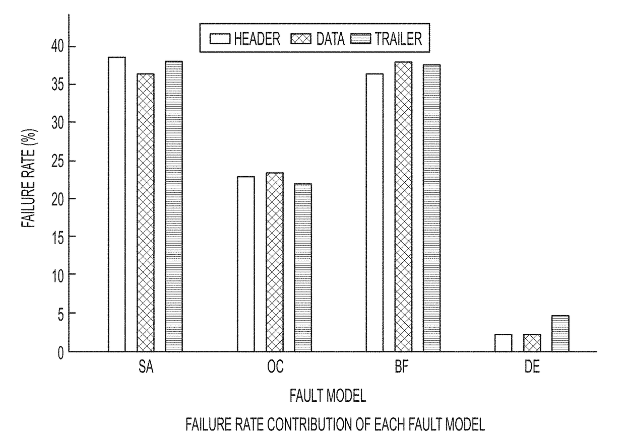
These effects include header / data flit loss, packet drop, packet truncation, packet latency, misrouting, timing
jitter, flit corruption, and disconnection.
A packet might never reach its expected destination, if a header loss occurs.
Packet latency: Packet latency is the result of the
router arbitration malfunction because of a fault inside the
arbiter logic, internal connections, or TSV connections.
TSV issues and some of the thermal related faults may change the
conductivity of TSVs or internal links by changing their physical structures.
Permanent faults in a routing unit component result in extra number of packet transmissions between adjacent routers and consequently causing congestion in some parts of the network.
It is a significant, and usually undesired, factor in the design of almost all communications links.
The delay caused by temperature variation and TSV coupling, leads to a timing
jitter, which is more significant for TSV because of its size.
Flit corruption: Flit corruption in a packet happens when a fault occurs in the
data path of a
router.
Disconnection: Different types of faults may cause the vertical link components (TSV body, contact, micro-bump) to fail.
However, there is a trade-off between the accuracy of the static
fault modeling and simulation time.
But the current version of TREAT reports an inconsistency of two simulation experiment, if the
signal values are not the same or they have same values in different timing slots.
THENoC is able to report these values but current version of TREAT does not provide other reliability
metrics independently.
Furthermore, the result of FIG. 5G shows how CTTC limits the maximum operational frequency of 3D NoCs.
In addition, these
capacitive coupling values can disrupt the timing requirement of a 3D IC based on the operational and TSV physical parameters.
Circuit-level simulation takes much longer than system-level simulation.
If the reported timing delay associated with the capacitive case violates the timing requirement of the
receiver logic, then the data bit is assumed faulty.
However, if the specified timing requirement of flip-flop tolerates the undesirable
propagation delay because of CTTC, then this fault will not have any
impact and it is ignored in the model.
Transient faults can be the major cause of failure in systems and they occur more frequently than permanent faults.
The reason is that the source-destination pairs of routers are not uniformly selected in FFT traffic.
The comparison shows that the accuracy of conventional
fault model for TSVs is substantially insufficient.
In other words, if the circuit-level simulations shows the 8 C capacitive coupling case results in failure the random
fault modeling is almost inaccurate for all the experiments.
However, inaccuracy percentages decrease as the factor of failing cases of parasitic capacitive reduces.
Consequently, the percentage of inaccuracy decreases for smaller parasitic capacitive causing failure.
It can be seen that the
data transmission from layer 2 downward layer 1 cause a large number of CTTC faults.
Although the baseline TCMA reduces the quantity of 8 C and 7 C
parasitic capacitance values, but it may have some undesirable side effects by converting a row of
data bits.
Based on the experimental result analysis, a bad configuration occurs in five cases, while two of them are potential to generate unwanted 8 C capacitive coupling and the other three may generate unwanted 7 C capacitive coupling.
This is because of the probability of bad configuration occurrence rises by increasing the sizes of TSV meshes.
Although the capacitive coupling is a well known source of
noise in TSV-based 3D ICs,
inductive coupling has also some undesirable effects like overshooting and supply / ground bounces.
As technology advances and supply
voltage shrinks, the coupled voltage becomes a greater portion of the Vdd and increases the
probability of error.
Consequently, the length of TSVs has a major
impact on
inductive coupling, resulting in unexpected noises in 3D NoC, as the number of
layers increases.
Shield
insertion on a chip and TSV placement with a safe distance approaches have been proposed to mitigate mutual coupling, but they are not efficient.
The overhead of this method is the extra bits, to decide the inversion process at the
receiver side.
There is a trade-off between the degree of inductive coupling mitigation and performance / complexity of the design.


