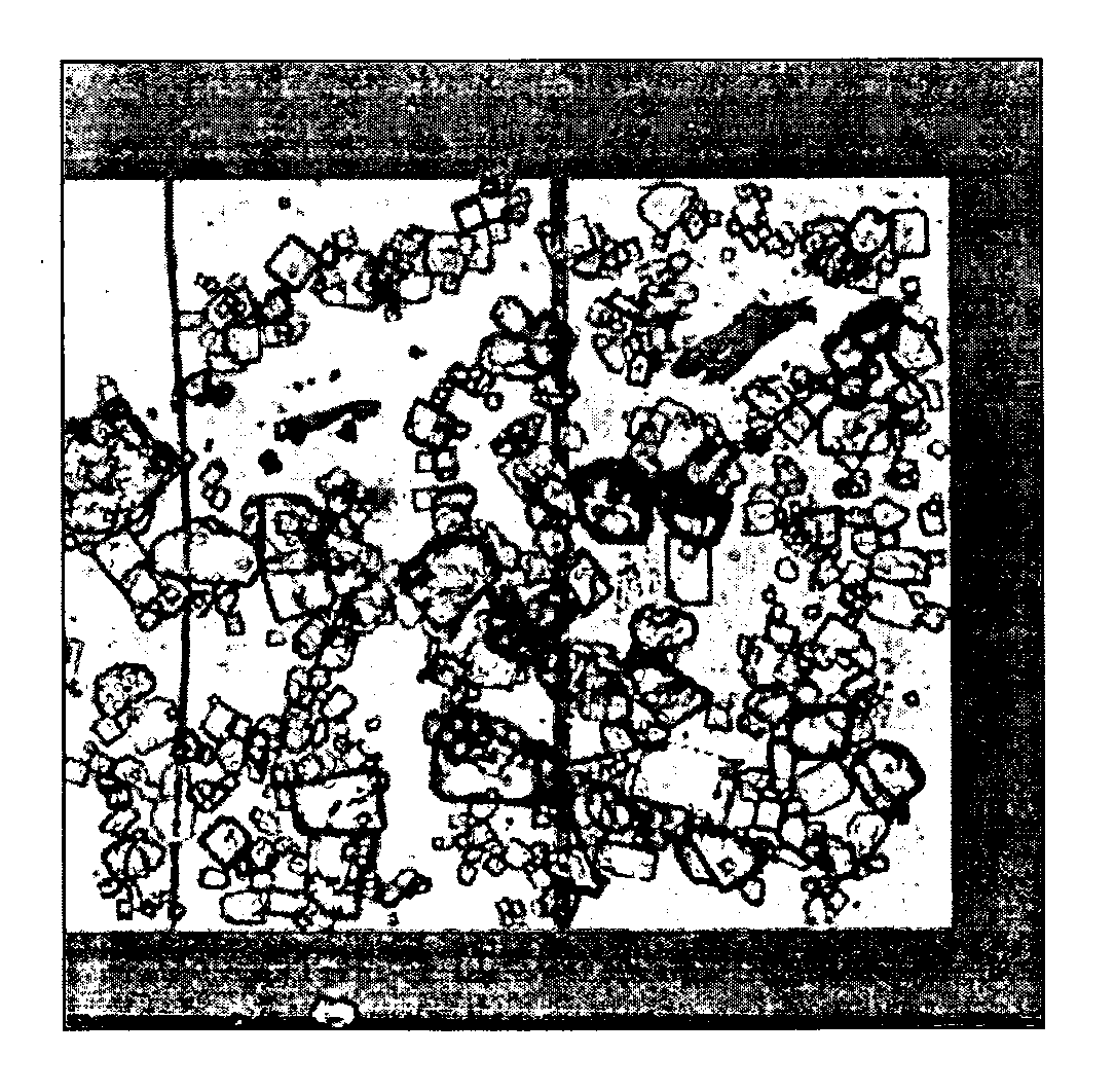
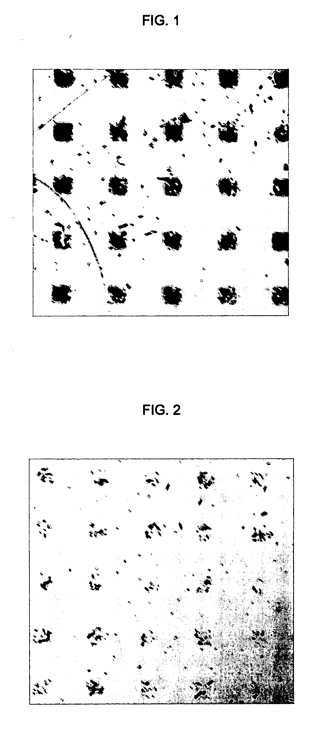
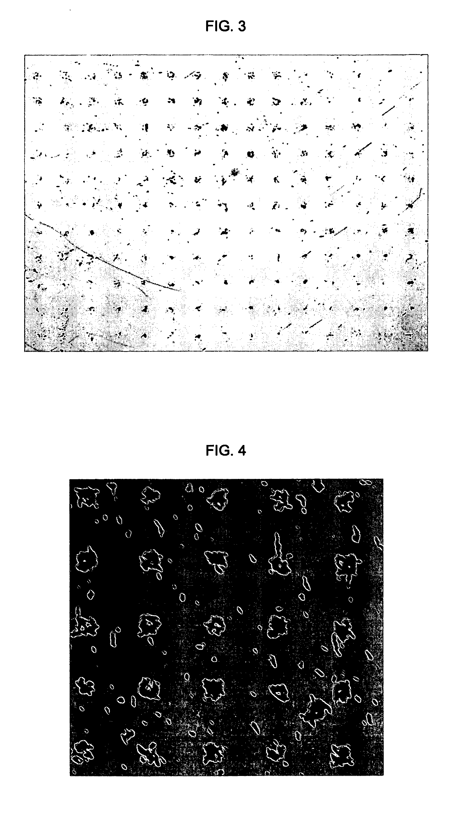
[0068] a) This method can be generally used for patterning objects of different materials irrespective of their size, surface properties, and morphologies.
[0070] c) This method is simple and cost-effective (no complicated design is required and valuable
crystal suspensions can be reused).
[0071] d) This method allows high yields as it allows patterns that can be covered with crystals up to 100%.
[0072] e) Potential control of
crystal orientation (e.g. by choosing patterns with appropriate shapes, crystals with appropriate dimensions and / or by control of the flow direction of the
crystallite suspension)
crystal alignment might be realized.
[0073] f) This method enables a reduction of
pollution as water or liquid mediums containing a major amount of water can be used for dispersing the crystals.
[0074] Any material that allows patterning of its surface with at least one compound (C1) can be used as the substrate. Preferred substrates are selected from materials suitable for the production of
semiconductor devices. Suitable substrates include, for example, metals (preferably metals of groups 8, 9, 10 or 11 of the
periodic table, e.g. Au, Ag, Cu), oxidic materials (like glass,
quartz, ceramics, SiO2), semiconductors (e.g. doped Si, doped Ge),
metal alloys (e.g. on the basis of Au, Ag, Cu, etc.),
semiconductor alloys, polymers (e.g. polyvinylchloride, polyolefines, like
polyethylene and
polypropylene, polyesters, fluoropolymers, polyamides, polyurethanes, polyalkyl(
meth)acrylates,
polystyrene and mixtures and composites thereof), inorganic solids (e.g.
ammonium chloride), and combinations thereof. The substrate can be a flexible or inflexible
solid substrate with a curved or planar geometry, depending on the requirements of the desired application.
[0075] A typical substrate for semiconductor devices comprises a matrix (e.g.
quartz or
polymer matrix) and, optionally, a
dielectric top layer (e.g. SiO2). The substrate also generally includes electrodes, like the drain and source electrodes of the OFETs, which are usually located on the substrate (e.g. deposited on the nonconductive surface of the
dielectric top layer). The substrate also includes conductive gate electrodes of the OFETs that are typically located below the
dielectric top layer (i.e., the
gate dielectric). According to a special embodiment, the drain and source electrodes are deposited partially on the
organic semiconductor crystallite rather than only on the substrate. Of course, the substrate can contain further components that are usually employed in semiconductor devices or ICs, such as insulators, resistive structures, capacitive structures,
metal tracks, etc.
[0076] The compound (C1) usually comprises at least one functional group capable of interaction with the surface of the substrate and also at least one functional group capable of interaction with the semiconductor compound. The functional groups capable of interaction with the surface of the substrate can be the same as the functional groups capable of interaction with the semiconducting compound. Alternatively, the compound (C1) can comprise two different species of functional groups, one for the interaction with the substrate and the other for the interaction with (S).
[0079] The expressions “
alkyl” and “alkylene” also comprise substituted
alkyl groups which can generally bear 1, 2, 3, 4 or 5 substituents, preferably 1, 2 or 3 substituents and particularly preferably 1
substituent, selected from among cycloalkyl,
aryl, hetaryl,
halogen, hydroxy,
thiol, NE1E2, NE1E2E3+, COOH,
carboxylate, —SO3H and
sulfonate.
[0078] In the following, the expression “
alkyl” comprises straight-chain and branched alkyl groups. These groups are preferably straight-chain or branched C1-C20-alkyl groups, more preferably C1-C12-alkyl groups, particularly preferably C1-C8-alkyl groups and most preferably C1-C4-alkyl groups. Examples of alkyl groups are, in particular, methyl, ethyl, propyl,
isopropyl, n-butyl, 2-butyl, sec-butyl, tert-butyl, n-pentyl, 2-pentyl, 2-methylbutyl, 3-methylbutyl, 1,2-dimethylpropyl, 1,1-dimethylpropyl, 2,2-dimethylpropyl, 1-ethylpropyl, n-hexyl, 2-hexyl, 2-methylpentyl, 3-methylpentyl, 4-methylpentyl, 1,2-dimethylbutyl, 1,3-dimethylbutyl, 2,3-dimethylbutyl, 1,1-dimethylbutyl, 2,2-dimethylbutyl, 3,3-dimethylbutyl, 1,1,2-trimethylpropyl, 1,2,2-trimethylpropyl, 1-ethylbutyl, 2-ethylbutyl, 1-ethyl-2-methylpropyl, n-heptyl, 2-heptyl, 3-heptyl, 2-ethylpentyl, 1-propylbutyl. n-octyl, 2-ethylhexyl, 2-propylheptyl, nonyl, decyl. Suitable longer-chain C8-C30-alkyl or C8-C30-alkenyl groups are straight-chain and branched alkyl or alkenyl groups. octyl(ene), nonyl(ene), decyl(ene), undecyl(ene), dodecyl(ene), tridecyl(ene), tetradecyl(ene), pentadecyl(ene), hexadecyl(ene), heptadecyl(ene), octadecyl(ene) and nonadecyl(ene) etc.
[0079] The expressions “alkyl” and “alkylene” also comprise substituted alkyl groups which can generally bear 1, 2, 3, 4 or 5 substituents, preferably 1, 2 or 3 substituents and particularly preferably 1
substituent, selected from among cycloalkyl,
aryl, hetaryl,
halogen, hydroxy,
thiol, NE1E2, NE1E2E3+, COOH,
carboxylate, —SO3H and
sulfonate.
[0080]“Cycloalkyl” is preferably C5-C8-cycloalkyl, such as cyclopentyl, cyclohexyl, cycloheptyl or cyclooctyl.
[0081] For the purposes of the present invention, the term “heterocycloalkyl” includes saturated, cycloaliphatic groups with in general 4 to 7, preferably 5 or 6, ring atoms in which 1 or 2 of the ring carbon atoms are replaced by heteroatoms chosen from the elements
oxygen,
nitrogen and
sulfur and which may optionally be substituted where, as in the case of a substitution, these heterocycloaliphatic groups may carry 1, 2 or 3, preferably 1 or 2, particularly preferably 1,
substituent chosen from alkyl,
aryl, COORa, COO-M+ and NE1E2, preferably alkyl.
[0082] Examples of heterocycloaliphatic groups which may be mentioned are pyrrolidinyl, piperidinyl, 2,2,6,6-tetramethylpiperidinyl, imidazolidinyl, pyrazolidinyl, oxazolidinyl, morpholidinyl, thiazolidinyl, isothiazolidinyl, isoxazolidinyl, piperazinyl, tetrahydrothiophenyl, tetrahydrofuranyl, tetrahydropyranyl and dioxanyl.
[0079] The expressions “alkyl” and “alkylene” also comprise substituted alkyl groups which can generally bear 1, 2, 3, 4 or 5 substituents, preferably 1, 2 or 3 substituents and particularly preferably 1 substituent, selected from among cycloalkyl, aryl, hetaryl,
halogen, hydroxy,
thiol, NE1E2, NE1E2E3+, COOH,
carboxylate, —SO3H and
sulfonate.
[0084]“Hetaryl” is preferably pyrrolyl, pyrazolyl, imidazolyl, indolyl, carbazolyl, pyridyl, quinolinyl, acridinyl, pyridazinyl, pyrimidinyl or pyrazinyl.
[0085] The groups NE1E2 are preferably N,N-dimethylamino, N,N-diethylamino, N,N-dipropylamino, N,N-diisopropylamino, N,N-di-n-butylamino, N,N-di-t-butylamino, N,N-dicyclohexylamino or N,N-diphenylamino.
[0084]“Hetaryl” is preferably pyrrolyl, pyrazolyl, imidazolyl, indolyl, carbazolyl, pyridyl, quinolinyl, acridinyl, pyridazinyl, pyrimidinyl or pyrazinyl.
[0093] In a second preferred embodiment the compound (C1) is bound to the surface of the substrate and / or to the crystalline compound (in particular (S)) via ionic interactions. According to this embodiment, the compound (C1) comprises at least one functional group capable of ionic interaction with the surface of the substrate and / or a compound (S).
[0088] Suitable functional groups for covalent interactions are preferably selected from hydroxyl, primary and secondary amino, thiol,
carboxylic acid,
carboxylic ester,
carboxamide, carboxylic anhydride,
sulfonic acid, sulfonic ester,
isocyanate, blocked
isocyanate, urethane,
urea,
ether, and
epoxy groups.
[0090] Table 1 exemplifies suitable pairs of complementary functional groups TABLE 1complementary functional groupsreactive group Rcomplementary(
meth)
acrylate / group R′isocyanatevinyl—SH—NH2—OH—CHOepoxyisocyanateX*XXX(
meth)acrylateXXXvinylXXX—SHXXXX—NH2XXXX—OHXXX—COOHXepoxyXXX—CHOXX
[0103] In a further preferred embodiment the compound (C1) is selected from mercaptocarboxylic acids, mercaptosulfonic acids and the
alkali metal or ammonium salts thereof. Examples of these compounds are
mercaptoacetic acid, 3-
mercaptopropionic acid, mercaptosuccinic acid, 3-mercapto-1-propanesulfonic acid and the alkali
metal or ammonium salts thereof, e.g. the
sodium or
potassium salts. These compounds are suiteable for a
hydrophilization of the surface of more hydrophobic substrates.
[0093] In a second preferred embodiment the compound (C1) is bound to the surface of the substrate and / or to the crystalline compound (in particular (S)) via ionic interactions. According to this embodiment, the compound (C1) comprises at least one functional group capable of ionic interaction with the surface of the substrate and / or a compound (S).
[0093] In a second preferred embodiment the compound (C1) is bound to the surface of the substrate and / or to the crystalline compound (in particular (S)) via ionic interactions. According to this embodiment, the compound (C1) comprises at least one functional group capable of ionic interaction with the surface of the substrate and / or a compound (S).
[0094] In a third preferred embodiment the compound (C1) is bound to the surface of the substrate and / or to the crystalline compound (in particular (S)) via
dipole interactions, e.g. van der Waals forces.
[0095] The interaction between (C1) and the substrate and / or between (C1) and the crystalline compound is preferably an attractive hydrophilic-hydrophilic interaction or attractive hydrophobic-hydrophobic interaction. Hydrophilic-hydrophilic interaction and hydrophobic-hydrophobic interaction can comprise, among other things, the formation of
ion pairs or
hydrogen bonds and may involve further van der Waals forces. Hydrophilicity or hydrophobicity is determined by affinity to water. Predominantly hydrophilic compounds or material surfaces have a high level of interaction with water and generally with other hydrophilic compounds or material surfaces, whereas predominantly hydrophobic compounds or materials are not wetted or only slightly wetted by water and aqueous liquids. A suitable measure for assessing the hydrophilic / hydrophobic properties of the surface of a substrate is the measurement of the
contact angle of water on the respective surface. According to the general definition, a “hydrophobic surface” is a surface on which the
contact angle of water is >90°. A “hydrophilic surface” is a surface on which the
contact angle with water is <90°. Compounds or material surfaces modified with hydrophilic groups have a smaller contact angle than the unmodified compound or materials. Compounds or material surfaces modified with hydrophobic groups have a larger contact angle than the unmodified compounds or materials.
[0096] Suitable hydrophilic groups for the compounds (C1) (as well as (C2) and / or (S)) are those selected from ionogenic, ionic, and non-ionic hydrophilic groups. Ionogenic or ionic groups are preferably
carboxylic acid groups,
sulfonic acid groups,
nitrogen-containing groups (amines), carboxylate groups, sulfonate groups, and / or quaternized or protonated
nitrogen-containing groups. Suitable non-ionic hydrophilic groups are e.g. polyalkylene
oxide groups. Suitable hydrophobic groups for the compounds (C1) (as well as (C2) and / or (S)) are those selected from the aforementioned
hydrocarbon groups. These are preferably alkyl, alkenyl, cycloalkyl, or aryl radicals, which can be optionally substituted, e.g. by 1, 2, 3, 4, 5 or more than 5
fluorine atoms.
[0103] In a further preferred embodiment the compound (C1) is selected from mercaptocarboxylic acids, mercaptosulfonic acids and the alkali metal or ammonium salts thereof. Examples of these compounds are
mercaptoacetic acid, 3-
mercaptopropionic acid, mercaptosuccinic acid, 3-mercapto-1-propanesulfonic acid and the alkali metal or ammonium salts thereof, e.g. the
sodium or
potassium salts. These compounds are suiteable for a
hydrophilization of the surface of more hydrophobic substrates.
[0098] In order to modify the surface of the substrate with a plethora of functional groups it can be activated with acids or bases. Further, the surface of the substrate can be activated by oxidation,
irradiation with
electron beams or by
plasma treatment. Further, substances comprising functional groups can be applied to the surface of the substrate via
chemical vapor deposition (CVD).
[0103] In a further preferred embodiment the compound (C1) is selected from mercaptocarboxylic acids, mercaptosulfonic acids and the alkali metal or ammonium salts thereof. Examples of these compounds are mercaptoacetic acid, 3-mercaptopropionic acid, mercaptosuccinic acid, 3-mercapto-1-propanesulfonic acid and the alkali metal or ammonium salts thereof, e.g. the sodium or potassium salts. These compounds are suiteable for a hydrophilization of the surface of more hydrophobic substrates.
[0100]
silanes, phosphonic acids, carboxylic acids, and hydroxamic acids: Suitable compounds (C1) comprising a
silane group are alkyltrichlorosilanes, such as n-(octadecyl)
trichlorosilane (OTS); compounds with trialkoxysilane groups, e.g. trialkoxyaminoalkylsilanes like triethoxyaminopropylsilane and N[(3-triethoxysilyl)propyl]ethylendiamine; trialkoxyalkyl-3-glycidylethersilanes such as triethoxypropyl-3-glycidylethersilane; trialkoxyallylsilanes such as allyltrimethoxysilane; trialkoxy(isocyanatoalkyl)
silanes; trialkoxysilyl(meth)acryloxyalkanes and trialkoxysilyl(meth)acrylamidoalkanes, such as 1-triethoxysilyl-3-acryloxypropan. (These groups are preferably employed to bind to metal
oxide surfaces such as
silicon dioxide,
aluminium oxide,
indium zinc oxide,
indium tin oxide and
nickel oxide.),
[0101] amines, phosphines and
sulfur containing functional groups, especially thiols: (These groups are preferably employed to bind to metal substrates such as gold, silver,
palladium,
platinum and
copper and to semiconductor surfaces such as
silicon and
gallium arsenide.)
[0097] Further suitable functional groups of the compounds (C1) are also ligand groups, capable of coordinating metal ions that can form additional coordinative bonds to the substrate and or (S). Functional groups suitable as ligands are e.g. carboxylic groups, hydroxyl groups, amino groups,
SH groups,
oxime groups,
aldehyde groups, keto groups and heterocyclic groups like
pyridine, chinoline,
imidazole or
oxazole.
[0101] amines, phosphines and
sulfur containing functional groups, especially thiols: (These groups are preferably employed to bind to metal substrates such as gold, silver,
palladium,
platinum and
copper and to semiconductor surfaces such as
silicon and
gallium arsenide.)
[0102] In a preferred embodiment, the compound (C1) is selected from C8-C30-alkylthiols and is in particular
hexadecane thiol. These compounds enable the application of crystallites of organic semiconducting compounds (S) to the surface of more hydrophobic substrates, such as Au (
water contact angle 65°) as well as more hydrophilic substrates such as NH4Cl (
water contact angle 49°).
[0103] In a further preferred embodiment the compound (C1) is selected from mercaptocarboxylic acids, mercaptosulfonic acids and the alkali metal or ammonium salts thereof. Examples of these compounds are mercaptoacetic acid, 3-mercaptopropionic acid, mercaptosuccinic acid, 3-mercapto-1-propanesulfonic acid and the alkali metal or ammonium salts thereof, e.g. the sodium or potassium salts. These compounds are suiteable for a hydrophilization of the surface of more hydrophobic substrates.
[0104] In a further preferred embodiment the compound (C1) is selected from alkyltrichlorosilanes, and is in particular n-(octadecyl)
trichlorosilane (OTS). These compounds enable the application of crystallites of organic semiconducting compounds (S) to the surface of more hydrophobic substrates, such as SiO2 (
water contact angle >100°).
[0105] Additionally to or as an alternative to deposition of said compound (C1) on the substrate, the substrate can be contacted with at least one compound (C2) capable of binding to the surface of the substrate as well as of interaction with the organic semiconducting compound (S) to prevent deposition of (S) on areas of the substrate not patterned with compound (C1).
[0106] According to a first embodiment, the compounds (C2) can be selected from the group of the aforementioned compounds (C1). Whether a particular compound acts as (C1) or as (C2) depends on the strength of interaction with the crystalline compound. It is of critical importance that the strength of the binding interaction of (C1) and (C2) with (S) differs to a sufficient degree so that (S) is essentially deposited on substrate areas patterned with (C1).
[0107] According to a further embodiment, the compounds (C2) are selected from compounds with a repulsive hydrophilic-hydrophobic interaction with (S). Suitable functional groups for repulsive interaction with certain compounds (S) are
hydrocarbon groups and (partially or fully) halogenated
hydrocarbon groups. The hydrocarbon or the halogenated hydrocarbon can be purely aliphatic or aromatic or can have a combination of aliphatic and aromatic groups. Halogenated hydrocarbons can bear one or more than one (e.g. 2,3,4,5 or more than 5) of the following halogen groups:
fluorine,
chlorine,
bromine,
iodine, or a combination thereof. Preferably, the partially or fully halogenated hydrocarbon is a partially or fully fluorinated hydrocarbon or a
chlorofluorocarbon. The hydrocarbon or the halogenated hydrocarbon can optionally bear further substituents apart from halogen.
[0108] As mentioned before the invention provides in a first embodiment a method of patterning the surface of a substrate with at least one crystalline compound, comprising the step of depositing on the surface of the substrate at least one compound (C1) capable of binding to the surface of the substrate and of binding at least one crystalline compound. According to this embodiment, preferably at least 90 % by weight, more preferably at least 95% by weight, especially at least 99% by weight, of the crystalline compound bound to the surface of the substrate is bound to surface areas patterned with (C1) (and not to unpatterned areas of the substrate or, if present, areas of the substrate coated with (C2)).
[0109] The second embodiment is a method of patterning the surface of a substrate with at least one crystalline compound, comprising the step of depositing on the surface of the substrate at least one compound (C2) capable of binding to the surface of the substrate and to prevent binding of a crystalline compound. According to this embodiment, preferably at least 90 % by weight, more preferably at least 95% by weight, especially at least 99% by weight, of the crystalline compound bound to the surface of the substrate is bound to surface areas not patterned with (C2) (i.e. to unpatterned areas of the substrate or, if present, areas of the substrate coated with (C1)).
[0110] Useful
organic semiconductor compounds (S) are in principle those known to the person skilled in the art. These include acenes such as
anthracene,
tetracene,
pentacene, and substituted acenes. A preferred
acene is
rubrene (5,6,11,12-tetraphenylnaphthacene). Substituted
acene compounds useful as organic semiconductors in the present invention preferably comprise at least one substituent selected from the group consisting of
electron-donating substituents (for example, alkyl, alkoxy, ester, carboxylate or thioalkoxy),
electron withdrawing substituents (for example halogen, nitro or cyano) and combinations thereof. Useful substituted pentacenes are e.g. 2,9-dialkylpentacenes and 2,10-dialkylpentacenes, wherein the alkyl group has from 1 to 12 carbons, 2,1 0-dialkoxypentacenes, and 1,4,8,11 -tetraalkoxypentacenes. Suitable substituted pentacenes are described in U.S. Published Appln. No. 2003 / 0100779, and U.S. Pat. No. 6,864,396. Examples of further useful organic semiconductors include perylenes, fullerenes, phthalocyanines, oligothiophenes, and substituted derivatives thereof. Suitable oligothiophenes are quaterthiophene, quinquethiophene, sexithiophene, α,ω-di(C1-C8)-alkyloligothiophenes, such as α,ω-dihexylquaterthiophene, α,ω-dihexylquinquethiophene and α,ω-dihexylsexithiophene, poly(alkylthiophenes) such as poly(3-hexylthiophene), bis(dithienothiophene), anthradithiophene and dialkylanthradithiophenes such as dihexylanthradithiophene,
phenylene-
thiophene (P-T) oligomers and derivatives thereof, especially a,co-alkyl substituted
phenylene-
thiophene oligomers such as tert. butyl-P-T-T-P-tert. butyl
oligomer. Examples of further useful organic semiconductors include
polyacetylene, polythienylenevinylene, C60. Especially preferred are
copper(II)
phthalocyanine and
rubrene.
[0111] For binding interaction with (C1) and / or repulsive interaction with (C2) the semiconductors (S) can be subjected to a reaction to introduce functional groups capable of such an interaction. Suitable functional groups for covalent, ionic bonds, van der Waals, coordinative and other interactions are the aforementioned groups of component (C2).
[0112] These groups can be introduced into the compounds (S) by e.g. reaction with functional groups of (S) that are capable of a
condensation reaction or
addition reaction and at least one compound selected from compounds that bear at least one functional group complementary to those groups of (S), wherein the compounds also bear at least one functional group capable of interacting with (C1) and / or (C2). In many cases it is not necessary to subject the semiconductors (S) to a functionalization, as compounds (C1) and, optionally, (C2) capable of interacting with the surface of the substrate and (S) are readily available. So e.g. the aforementioned C8-C30-alkylthiols (C1) and, in particular,
hexadecane thiol, are capable of attracting compounds (S) bearing hydrocarbon groups, e.g. aromatic rings or alkyl chains.
[0113] According to the invention, the
organic semiconductor compound (S) is employed in the form of crystallites. For the purpose of the invention, the term “
crystallite” refers to small single crystals with maximum dimensions of 5 millimeters. Exemplary crystallites have maximum dimensions of 1 mm or less and preferably have smaller dimensions (frequently less than 500 μm, in particular less than 200 μm, for example in the range of 0.01 to 150 μm, preferably in the range of 0.05 to 100 μm), so that such crystallites can form fine patterns on the substrate. Here, an individual crystallite has a single crystalline domain, but the domains may include one or more cracks, provided that the cracks do not separate the crystallite into more than one crystalline domain. The stated particle sizes and the christallographic properties of the crystallites can be determined by direct X-
ray analysis.
[0114] The particles of the semiconductor compound (S) may be of regular or
irregular shape. For example, the particles can be present in spherical or virtually
spherical form or in the form of needles.
[0115] Preferably the organic semiconductor (S) is employed in the form of particles with a length /
width ratio (L / W) of at least 1.05, more preferably of at least 1.5, especially of at least 3.
[0117]
Organic semiconductor crystallites, e.g. with diameters of about 1 to 10 microns or more, are readily available. Such organic semiconductor crystallites can be fabricated by methods described by R. A. Laudise et al in “Physical
vapor growth of organic semiconductors” Journal of
Crystal Growth 187 (1998) pages 449-454 and in “Physical
vapor growth of
centimeter-sized crystals of a-hexathiophene” Journal of
Crystal Growth 182 (1997) pages 416-427. Both of these articles by Laudise et al are incorporated herein in their entirety by reference. The methods described by Laudise et al include passing an
inert gas over an organic semiconductor substrate that is maintained at a temperature high enough that the organic semiconductor evaporates. The methods described by Laudise et al also include
cooling down the gas saturated with organic semiconductor to cause an organic semiconductor crystallite to condense spontaneously. Such organic semiconductor crystallites are also commercially available. For example, BASF Corporation of 3000 Continental Drive-North,
Mount Olive, N.J. 07828-1234, sells
pigment crystallites that are organic semiconductors. One such crystallite is formed of
copper phthalocyanine. The ready availability of organic semiconductor crystallites enables the construction of OFETs with high quality channels.
[0118] In step a) of the process according to the invention, a stamp, having a surface including a plurality of indentations defining an indentation pattern formed therein, said indentations being contiguous with a stamping surface and defining a stamping pattern, is provided.
[0119] Stamps useful in the present invention are known in the art and are commercially available. Generally, these stamps can be produced by
casting a polymeric material onto a mold having the desired pattern. The particular material chosen for formation of the stamp is not critical to the present invention, but should satisfy certain physical characteristics. In a preferred embodiment, the stamp is elastomeric. Polymeric materials suitable for use in fabrication of the stamp may have linear or branched backbones, and may be crosslinked or noncrosslinked, depending upon the particular
polymer and the degree of
formability desired of the stamp. A variety of elastomeric polymeric materials are suitable for such fabrication, especially polymers of the general classes of
silicone polymers,
epoxy polymers, and
acrylate polymers. Examples of
silicone elastomers suitable for use as stamps include those formed from precursors including the chlorosilanes such as methylchlorosilanes, ethylchlorosilanes, and phenylchlorosilanes, and the like. A particularly preferred
silicone elastomer is
polydimethylsiloxane (PDMS). Exemplary silicone polymers include those sold under the
trademark RTV by GE
Advanced Materials and under the
trademark Sylgard by the Dow Chemical Company, Midland, Mich., and particularly Sylgard 182, Sylgard 184, and Sylgard 186.
[0120] The stamp includes a stamping surface having a variety of features defined thereon by indentations. The form and dimensions of the indentations depend on the nature of the electronic devices to be formed on the substrate (e.g. molecular-sized transistors, connecting wires, etc.). Accordingly, the stamping surface may include features having a variety of lateral dimensions. Different patterns on the substrate can be obtained by the process of the invention. The elevations of the stamp defining the stamping pattern can have the same or different forms. Preferably the indentations are uniform and are e.g. in the form of a polygon, having 3, 4, 5, 6, 7, 8, 9, 10, 11 or 12 corners. Preferably, the indentations are rectangular, ellipsoidal or circular. Each indentation can have a minimum dimension of at least 50 nm, preferably at least 100 nm, more preferably at least 500 nm. Each indentation can have a
maximum dimension of up to 5 mm, preferably of up to 1 mm, more preferably of up to 500 μm. Typical indentations are in the form of 10 μm-100 μm squares, 5-100 μm lines, and 10 -100 μm dots. The distance between two adjacent indentations is preferably at least 50 nm, more preferably at least 100 nm, especially at least 500 nm.
[0121] A suitable method for forming the stamp is a photolytic method. For example, a
mask may be positioned between the surface of the stamp and a source of
irradiation, and the surface is irradiated through the
mask for a predetermined period of time. Portions of the surface may be degraded by such
irradiation, forming indentations in the surface upon removal of such degraded portions. According to this method, a variety of patterns may be very conveniently formed in a stamp according to a variety of available masks. In addition, the photolytic method may be used in combination with the above-described methods involving hardening a hardenable fluid on a mold surface. For example, a hardenable fluid may be contacted with a mold surface and allowed to harden to form the stamp having a predetermined stamping surface. In addition, the predetermined stamping surface may be irradiated through a
mask to create additional features in the stamping surface. According to this method, a
photoresist may be used as the stamp material itself. Particular types of polymers that may be patterned using the above-described photolytic method, preferred wavelengths for photopatterning, and lengths of time of photolysis are known in the art.
[0122] The surface of the mold serving as the master for the stamp may comprise any morphological features that may desirably serve as a template for the formation of the stamp for the patterning of a semiconductor on the surface of a substrate. For example, a microeletronic device such as an IC may serve as a template. The mold surface may be formed according to a variety of ways. According to one, the mold surface is micromachined from a material such as metal. According to another, the mold surface is formed lithographically by providing a substrate, depositing a film of material onto the substrate,
coating an exposed surface of the material with
resist, irradiating the
resist according to a predetermined pattern, removing irradiated portions of the
resist from the material surface, contacting the material surface with a reactant selected to react chemically therewith and selected to be chemically
inert with respect to the resist such that portions of the material according to the predetermined pattern are degraded, removing the degraded portions, and removing the resist to uncover portions of the material formed according to the predetermined pattern to form the mold surface. According to another method for forming the mold surface, a substrate may be provided, and coated with resist. Subsequently, portions of the resist may be irradiated according to a particular predetermined pattern. Irradiated portions of the resist may then be removed from the substrate to
expose portions of the
substrate surface according to the predetermined pattern, and the substrate may be contacted with a plating
reagent such that exposed portions according to the predetermined pattern are plated. Then, the resist may be removed to uncover portions of the exposed substrate according to the predetermined pattern bordered by plated portions of the substrate to form the mold surface.
[0123] In step b) of the process according to the invention, the stamping surface is coated with at least one compound (C1) or (C2) (i.e. the stamped being “inked” with at least one
compound C1 or C2). The stamp may be inked with a solution comprising the compounds (C1) or (C2) that will be adsorbed to the stamp. Accordingly, the inking may, e.g. be accomplished by: contacting the stamp with a material (i. e., paper,
sponge) moistened with the ink, pouring the ink directly onto the stamp, applying the ink to the stamp with an appropriate application device (e. g. a
cotton swab,
brush,
sprayer,
syringe, etc.), or dipping the stamp surface into a solution comprising (C1) or (C2). The compound may be allowed to dry on the stamp or may be blown dry.
[0124] In step c) of the process according to the invention, at least a portion of the surface of the substrate is contacted with the stamping surface to allow deposition of the compound (C1) or (C2) on the substrate.
[0125] The inked stamp is then placed into contact with the
functionalized polymer surface for a length of time sufficient for the compound (C1) or (C2) to be transferred to the surface of the substrate. The period of time required for the
stamping process will of course vary with the compounds (C1) and (C2), material of the stamp and substrate being used. A person skilled in the art will be able to determine a suitable amount of time. For example, contacting the stamping surface with the surface of the substrate for a period of time in the range of approximately 1 second to 5 minutes (e.g. 5 to 60 seconds) is generally adequate to effect sufficient transfer, but contact may be maintained for longer or shorter periods of time if necessary or appropriate.
[0126] In step d) of the process according to the invention, the stamping surface is removed to provide a pattern of binding sites on the surface of the substrate. These binding sites are capable of binding crystallites of the organic semiconductor compound (S) by the aforementioned mechanisms.
[0127] In one embodiment of the present invention, the substrate may be stamped more than once, e.g. to produce different types of binding sites on the surface of the substrate. The presence of different species of binding sites can be useful for the construction of complex circuits. For example, the different species of binding sites can be modified with different compounds (C1); thus, different semiconductors (S) can be bound to the substrate.
[0129] The substrate with a pattern of sites on the surface that prevent binding of a crystalline compound, obtained in step d) by the method according to the second embodiment of the invention, can optionally be contacted with at least one compound (C1) to allow deposition of the crystalline compound on areas of the substrate not patterned with compound (C2). As mentioned before, the compounds (C2) usually show a repulsive interaction with the compounds (C1) and the compounds (C1) are usually not capable of replacing or covering sites already covered with (C2). Therefore, (C1) can usually be applied to those substrates by contacting the surface of the substrate with a solution of at least one compound (C1) in a suitable
solvent. After a span of time sufficient to bind (C1) to the surface of the substrate, the solution is preferably removed from the substrate by rinsing with a
solvent. Of course, defined areas of the substrate can also be patterned with at least one compound (C1) by using the pattern technique for application of (C2).
[0129] The substrate with a pattern of sites on the surface that prevent binding of a crystalline compound, obtained in step d) by the method according to the second embodiment of the invention, can optionally be contacted with at least one compound (C1) to allow deposition of the crystalline compound on areas of the substrate not patterned with compound (C2). As mentioned before, the compounds (C2) usually show a repulsive interaction with the compounds (C1) and the compounds (C1) are usually not capable of replacing or covering sites already covered with (C2). Therefore, (C1) can usually be applied to those substrates by contacting the surface of the substrate with a solution of at least one compound (C1) in a suitable
solvent. After a span of time sufficient to bind (C1) to the surface of the substrate, the solution is preferably removed from the substrate by rinsing with a solvent. Of course, defined areas of the substrate can also be patterned with at least one compound (C1) by using the pattern technique for application of (C2).
[0130] Preferably, a suspension of
solid semiconductor particles in a
liquid medium is used for applying a plurality of crystallites of the organic semiconductor compound (S) to the surface of the substrate in step e).
[0131] Preferably, the semiconductor compound (S) has a
solubility in the
liquid medium of not more than 10 g / l, more preferably of not more than 5 g / l, especially of not more than 1 g / l at 25° C. / 1013 mbar.
[0132] The
liquid medium is preferably selected from water and mixtures of water and at least one water-miscible
organic solvent. Mixtures of water and at least one water water-miscible
organic solvent preferably contain not more than 20 % by weight of organic solvents. Suitable water-miscible organic solvents are C3-C4-ketones such as
acetone und methylethylketone, cyclic ethers such as dioxane and tetrahydrofurane, C1-C4-alkanoles such as
methanol,
ethanol, n-
propanol, isopropanol, n-
butanol, tert.-
butanol, polyoles and mono- und dimethylether thereof, such as Glycole,
propanediol,
ethylene-glycolmonomethylether, diethyleneglycol, Diethyleneglycolmonomethylether, diethyle-neglycoldimethylether,
glycerol, C2-C3-nitriles, like
acetonitrile und
propionitrile, di-methylsulfoxide,
dimethylformamide,
formamide,
acetamide,
dimethylacetamide, buty-rolacton, 2-pyrrolidone und N-methylpyrrolidone. Preferred as the liquid medium are mixtures of water and at least one C1-C4-alkanol.
[0130] Preferably, a suspension of
solid semiconductor particles in a liquid medium is used for applying a plurality of crystallites of the organic semiconductor compound (S) to the surface of the substrate in step e).
[0134] The solids content of the suspension is generally in the range of 0.001 to 20% by weight and in particular in the range of 0.1 to 10% by weight.
[0135] For the application of the crystallites of the organic semiconductor compound to the substrate, solution-based techniques such as pipetting, spin- or immersion-coating, i.e., dip-coating, can be used. In the case of pipetting, a suspension of the semiconductor crystallites is added dropwise to the
patterned substrate. In the case of spin-coating, the
patterned substrate is flooded with a suspension of the semiconductor crystallites and then spun to bring the substrate in intimate contact with the suspension. In the case of immersion-coating (dip-coating), the
patterned substrate is immersed in a suspension containing the semiconductor crystallites, preferably under agitation of the suspension, and then withdrawn from the suspension. In all of these cases, the liquid medium is preferably removed from the substrate after the application by rinsing with a solvent. Preferably, the solvent corresponds to the liquid medium of the suspension used for application of the crystallites. Afterwards, the solvent is removed, typically by spontaneous
evaporation. The rate of
evaporation can be accelerated by means of one or more methods known in the art such as heat, reduced pressure, ventilation, and the like.

